
Nvidia's custom HBM pulls Samsung onto TSMC's 3nm process, report says
DIGITIMESen
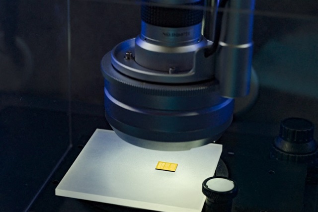
Nvidia's custom memory design is shifting control of how high-bandwidth memory (HBM) is built from memory makers to its largest customer, and steering a key part of that work to TSMC. Samsung Electronics, which has made every part of its HBM stacks in-house, has agreed after an internal review to use TSMC's 3nm process for the base die of NVHBM, Nvidia's next-generation custom HBM, the Seoul Economic Daily reported on October 18, citing industry sources. The newspaper said it would be the first time the two companies have worked together at the HBM manufacturing stage.
This is a short summary published by AI Global Wire. The full article is owned and hosted by DIGITIMES — open it there to read it in full.
Read the full story at DIGITIMES- Forskning
Related AI news
- ByteDance Seed launches AI safety team, global recruitment driveDIGITIMES · October 19, 2026
- Anthropic to commit 5% of shares to public benefit fundTech in Asia · October 19, 2026
- DeepSeek releases updated V4.1-Flash model it says completes tasks fasterSiliconANGLE · October 18, 2026
- Samsung to use TSMC technology for Nvidia's next-generation memory chips: ReportEconomic Times Tech · October 18, 2026
- Anthropic has nearly stopped hiring junior staff because AI agents now work six times as many hoursThe Decoder · October 18, 2026
- Only 8% of fund managers report improved investment returns from AI adoption: ReportEconomic Times Tech · October 18, 2026