
PLP splits roles as FOPLP focuses on cost and CoPoS courts AI chips
DIGITIMESen
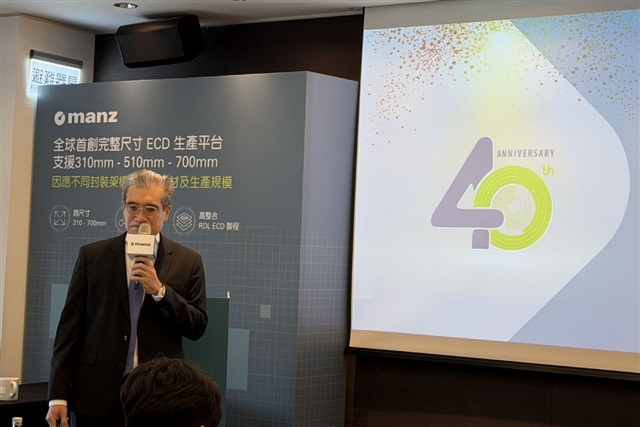
As AI chips move toward larger dies and higher integration, advanced packaging is shifting from 300mm wafers to square panel manufacturing. In panel-level packaging (PLP), FOPLP and CoPoS have emerged as the two hottest keywords, while glass-based technologies remain further ahead on the roadmap.
This is a short summary published by AI Global Wire. The full article is owned and hosted by DIGITIMES — open it there to read it in full.
Read the full story at DIGITIMESRelated AI news
- Artturi Sarvela, 24, ei saa oman alan töitä, kun kokemusta puuttuu – eikä kokemusta saa ilman töitäYle Uutiset · August 19, 2026
- Jane Street leads $700m raise for US AI chip startup EtchedTech in Asia · August 19, 2026
- Cerebras launches new server chip and system designed to speed AI chatbotsEconomic Times Tech · August 19, 2026
- 電力散熱一體化,Trane 攜伊頓攻 AI 資料中心TechNews (TW) · August 19, 2026
- “벤처 호황기마저 제쳤다”…상반기 신규 벤처투자 8.9조 '역대 최대'ETNews (KR) · August 19, 2026
- 金融時報:輝達 H200 晶片抵中國,助 AI 業者追趕美國TechNews (TW) · August 19, 2026