
Samsung chairman Lee Jae-yong turns to Japan for AI chip packaging edge
DIGITIMESen
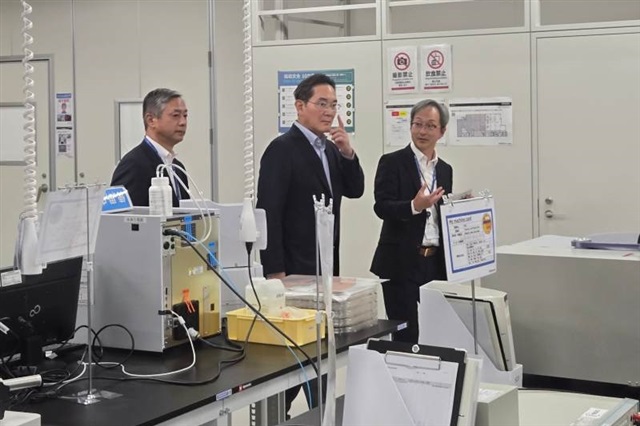
Samsung Electronics chairman Lee Jae-yong visited the company's Advanced Package Lab (APL) in Yokohama, Japan, on November 1, as the chipmaker looks to Japan's semiconductor materials and equipment industry to strengthen its advanced packaging capabilities for AI processors.
This is a short summary published by AI Global Wire. The full article is owned and hosted by DIGITIMES — open it there to read it in full.
Read the full story at DIGITIMESRelated AI news
- 韓國 2027 預算案規模 20 兆創新高,聚焦民生、AI 及國防TechNews (TW) · November 2, 2026
- Spielebranche: Claude darf keine bekannten Games mehr nachbauenGolem.de · November 2, 2026
- Linus Torvalds 釋出最新 Linux 核心 RC 版,肯定 AI 參與開發模式漸趨「健康」TechNews (TW) · November 2, 2026
- AI Agents Break Web Ad Model | Lightspeed’s Harsha, Hemant Mohapatra | Corner Office ConversationEconomic Times Tech · November 2, 2026
- HSBC to open Hong Kong AI Institute following Singapore launchEconomic Times Tech · November 2, 2026
- Suomalaisyritys yrittää ratkoa rakennusalan kipukohtaa tekoälyllä – Sai kasvuun miljoonatuenTivi · November 2, 2026