
Samsung diverges from TSMC on FOPLP: retains 415×510mm panel size, targets 2028 mass production
DIGITIMESen
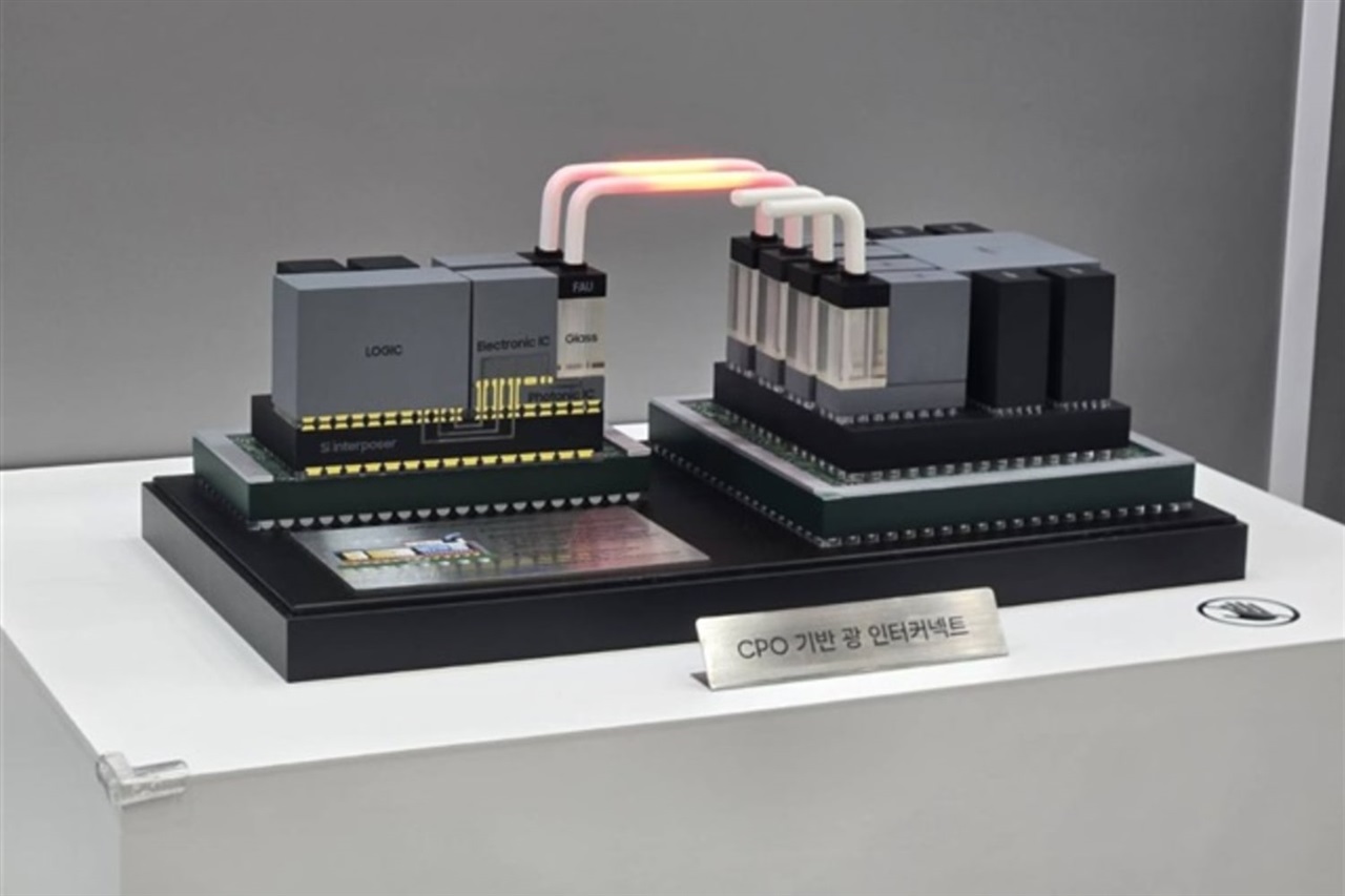
Samsung Electronics' packaging technology lead, Lee Hee-seok, outlined the company's advanced semiconductor packaging roadmap at Advanced Semiconductor Packaging & Chiplet Show (ASPS) 2026. Beyond sharing target production timelines and specifications for fan-out panel-level packaging (FOPLP) and glass substrates, Lee emphasized AI's pivotal role in driving packaging R&D forward.
This is a short summary published by AI Global Wire. The full article is owned and hosted by DIGITIMES — open it there to read it in full.
Read the full story at DIGITIMESRelated AI news
- Tekoäly teki huijauksista entistä kavalampia – Lähes joka kolmas suuryritys kokee maksupetosten lisääntyneenTivi · August 28, 2026
- Matt Lucas and Hugh Bonneville among actors calling for law on AI voice cloningBBC Technology · August 28, 2026
- Blogindlæg: Jeg skal med på Digitaliseringsmessen Del II – Svend Brinkmann stiller de spørgsmål vi glemte at stilleVersion2 · August 28, 2026
- Need spiritual guidance? Gurus join chatbot trend as people turn to AI for answersEconomic Times Tech · August 28, 2026
- Anthropic vs. Pentagon: US-Regierung handelte „rechtswidrig und unbegründet“heise online – KI · August 28, 2026
- SoftBank-backed surgical robotics firm eyes Hong Kong listing to power mainland China pushSCMP Tech · August 28, 2026