
Samsung's Lee bets on Japan for AI chip packaging edge
DIGITIMESen
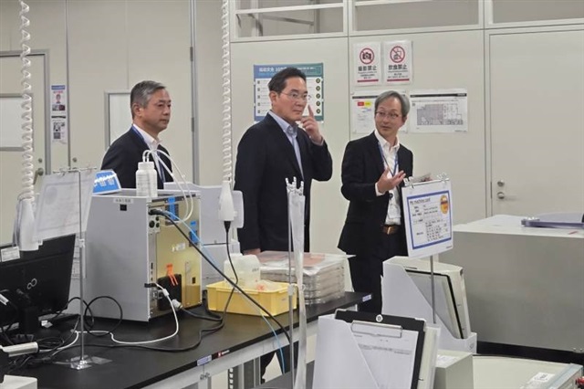
Samsung Electronics chairman Lee Jae-yong visited the company's Advanced Package Lab (APL) in Yokohama, Japan, on November 1, as the chipmaker looks to Japan's semiconductor materials and equipment industry to strengthen its advanced packaging capabilities for AI processors.
This is a short summary published by AI Global Wire. The full article is owned and hosted by DIGITIMES — open it there to read it in full.
Read the full story at DIGITIMESRelated AI news
- Anthropic sätter stopp för AI-kopior av populära spelComputer Sweden · November 2, 2026
- Filing: Anthropic plans to raise up to $3.5B from Japanese investors as part of its IPO, joining Australia, Canada, and parts of Europe in having direct access (Yasutaka Tamura/Bloomberg)Techmeme · November 2, 2026
- How Hong Kong’s fintech strategy is progressing – and where growth still lagsSCMP Tech · November 2, 2026
- Hundreds of Mundane AI Apps Are Hiding Sexually Abusive Deepfake FeaturesWIRED AI · November 2, 2026
- Professorer stempler Netcompanys AI-analyse som urealistisk: »Det er problematisk at lave den type business case«Ingeniøren · November 2, 2026
- Tekoälyn käyttäytymisessä havaittiin hälyttävä muutos: Oppi pahoille tavoille somestaTivi · November 2, 2026