
Samsung weighs Giheung R&D line for 2nm HBM foundry capacity
DIGITIMESen
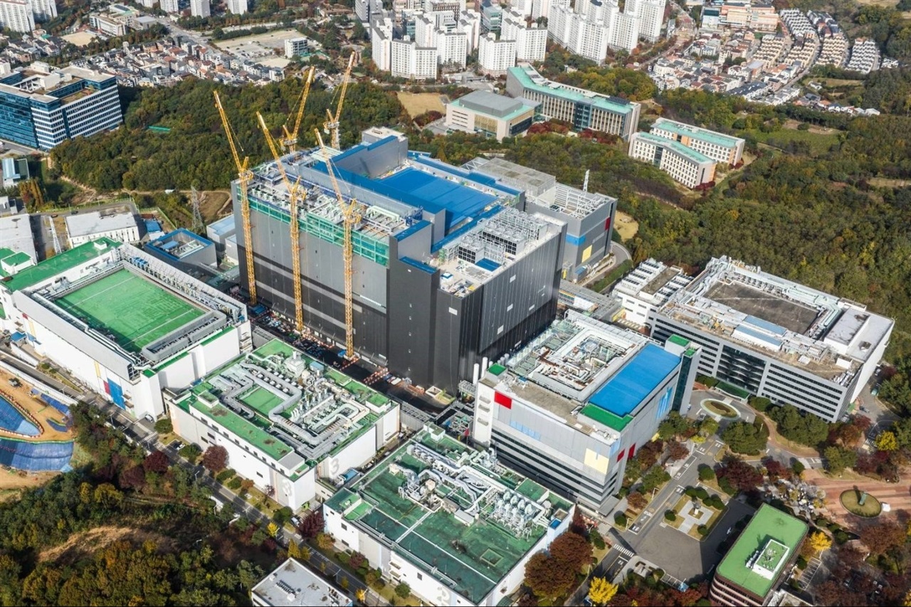
Samsung Electronics is reportedly considering repurposing the second line at its next-generation semiconductor R&D complex in Giheung into a foundry send-fab, a shift that would add advanced-node capacity as demand for AI memory strains leading-edge capacity.
This is a short summary published by AI Global Wire. The full article is owned and hosted by DIGITIMES — open it there to read it in full.
Read the full story at DIGITIMESRelated AI news
- 輝達變身 AI 央行?明星經理人 Baker:非循環融資TechNews (TW) · August 17, 2026
- 太空 AI 成保險業新藍海 但如何定價風險是挑戰TechNews (TW) · August 17, 2026
- 上線不到一年就退場,微軟將 Mico 移出 Copilot 語音功能TechNews (TW) · August 17, 2026
- Chinese robots on the march despite tech war hurdlesSCMP Tech · August 17, 2026
- Montag: Ringen um Daten insolventen Cloud-Providers, Datenklau bei Großkonzernenheise online – KI · August 17, 2026
- Anthropic's text watermark alters word probabilities to embed a fingerprint, which could degrade Claude's writing, despite its claim of no impact on quality (John Gruber/Daring Fireball)Techmeme · August 17, 2026