
SK Hynix advances chip inspection technology as 3D memory pushes conventional metrology to its limits
DIGITIMESen
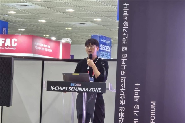
SK Hynix is strengthening its metrology and inspection (MI) capabilities as the transition toward 3D DRAM architectures and increasingly complex NAND stacking creates new challenges for conventional semiconductor inspection technologies.
This is a short summary published by AI Global Wire. The full article is owned and hosted by DIGITIMES — open it there to read it in full.
Read the full story at DIGITIMESRelated AI news
- TPCA 展明登場 PCB 產值今年破兆 / 材料吃緊延續TechNews (TW) · October 19, 2026
- heise+ | Home Assistant und KI: Was der Home Generative Agent wirklich kannheise online – KI · October 19, 2026
- OpenAI, Moderna expand AI use in drug developmentTech in Asia · October 19, 2026
- Stripe Link data shows agentic transactions increased by 38x and volume of payments by 20x in September, with retail leading in both, and a ~$100 average spend (Alex Konrad/Upstarts Media)Techmeme · October 19, 2026
- SG AI cloud provider Aolani eyes Malaysia data center dealsTech in Asia · October 19, 2026
- “바이오데이터 연구 활용…美는 일주일, 한국은 최소 1년”ETNews (KR) · October 19, 2026