
SK Hynix holds groundbreaking ceremony for $4 billion Indiana AI chip packaging facility
Economic Times Techen
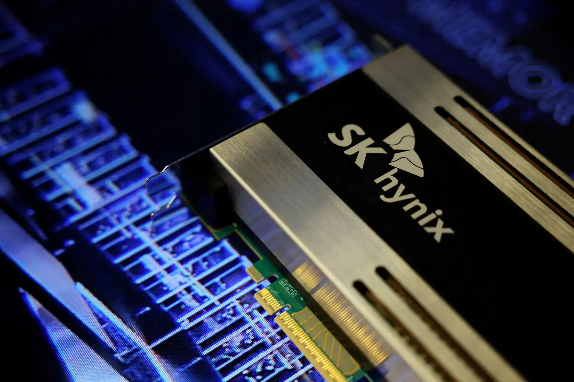
The facility, at the Purdue Research Park in West Lafayette, is scheduled to begin cleanroom operations in the second half of 2028, according to SK Hynix's website and press statements. The site will house a next-generation high-bandwidth memory (HBM) packaging line as well as an AI semiconductor research and development facility.
This is a short summary published by AI Global Wire. The full article is owned and hosted by Economic Times Tech — open it there to read it in full.
Read the full story at Economic Times Tech- Forskning
Related AI news
- OpenAI researcher warns ultrafast AI could leave security teams in the dustThe Decoder · August 27, 2026
- When agents act on their own, governance has to live in the data layerVentureBeat AI · August 27, 2026
- Cambridge, MA-based Transfyr emerges from stealth with a $25M seed to use AI to address science's reproducibility crisis and capture labs' "tacit knowledge" (Carl Zimmer/New York Times)Techmeme · August 27, 2026
- Anthropic releases findings from a pilot that let three external researchers run studies on Claude usage; one study found users delegate high-stakes tasks (Anthropic)Techmeme · August 27, 2026
- AI spots at-risk pregnancies for earlier, more personalized prenatal careNordic AI (EN) · August 27, 2026
- AI Begins to Wield Significant Influence on Consumers’ Auto and Home Insurance DecisionsAI Earnings (Google News) · August 27, 2026