
Applied Materials opens R&D center to speed chipmaking for the AI era
DIGITIMESen
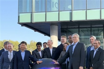
Applied Materials has opened its Equipment and Process Innovation and Commercialization (EPIC) Center in Sunnyvale, California, positioning the Silicon Valley site as a new hub for semiconductor research and manufacturing development. The company expects spending at the facility to rise over time to about US$5 billion as customer projects ramp up, underscoring how AI demand is reshaping the chip equipment industry.
This is a short summary published by AI Global Wire. The full article is owned and hosted by DIGITIMES — open it there to read it in full.
Read the full story at DIGITIMES- Verktyg
- Forskning
Related AI news
- AMD Helion aims to reshape data center design for agentic AIDIGITIMES · October 13, 2026
- Unexpected Claude test behavior prompts US govt to mandate AI incident reportingDIGITIMES · October 13, 2026
- Microsoft's 2nm Maia 300 completes cloud AI ASIC lineup, setting up 2027 server supply-chain boomDIGITIMES · October 13, 2026
- Le groupe Meta dévoile son nouveau modèle d’IA, Muse Wonder, censé rivaliser avec ChatGPT et ClaudeLe Monde Pixels · October 13, 2026
- Avec son nouveau modèle d’IA, Muse Wonder, le groupe Meta affirme rivaliser avec OpenAI et AnthropicLe Monde Pixels · October 13, 2026
- Applied Materials opens new $5B chip research facility to accelerate collaborative semiconductor innovationSiliconANGLE · October 13, 2026