
ASML patents point to a hybrid bonder as chip toolmakers crowd into packaging
DIGITIMESen
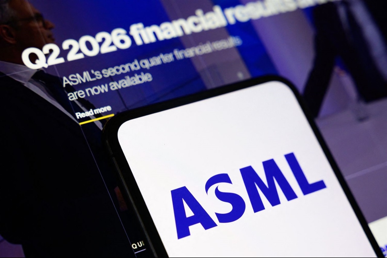
As it becomes harder and costlier to shrink transistors, advanced packaging has become the place chip equipment makers look to for their next leg of growth, and ASML appears to be preparing its second move into it. Patent filings analyzed by research firm SemiAnalysis suggest the Dutch lithography leader is building a die-to-wafer (D2W) hybrid bonder, a tool that would pit it against Besi, the current leader, and a growing group of front-end rivals chasing the same market.
This is a short summary published by AI Global Wire. The full article is owned and hosted by DIGITIMES — open it there to read it in full.
Read the full story at DIGITIMES- Verktyg
- Forskning
Related AI news
- OpenAI continues to work to grow its ad business in ChatGPT, cutting ad rates, chasing small and midsize businesses, and hiring some new talent from Meta (Alix Coutures/The Information)Techmeme · October 16, 2026
- AI agents on Tencent Cloud try to break into Alibaba’s Amap: researchersSCMP Tech · October 16, 2026
- Chinese chip toolmakers buy into hybrid bonding as Huawei looks beyond transistor shrinkingDIGITIMES · October 16, 2026
- Perplexity AI open-sources its secure AI agent sandbox SPACESiliconANGLE · October 16, 2026
- 8 insights from LogicMonitor’s Elevate event: AI-driven observability moves toward autonomous ITSiliconANGLE · October 16, 2026
- HK research arm Flair opens embodied AI applications hubTech in Asia · October 16, 2026